
Application of Ceramic Substrates in Third-Generation Semiconductor Power Device Packaging
- Iva Leung
- Feb 16, 2024
- 2 min read

The third-generation semiconductor typically refers to semiconductor materials with a bandgap wider than 2.2eV, also known as wide-bandgap semiconductor materials. The development of the semiconductor industry can be broadly divided into three stages: the first generation represented by silicon (Si), the second generation represented by gallium arsenide (GaAs), which has been widely used, and the third generation represented by wide-bandgap materials such as silicon carbide (SiC), gallium nitride (GaN), zinc oxide (ZnO), and diamond. These third-generation materials have gained rapid development in recent years due to their significant advantages over first- and second-generation materials.
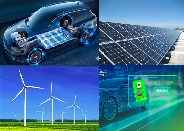
SiC, GaN, ZnO, and other third-generation semiconductors possess wider bandgaps, higher thermal conductivity, greater radiation resistance, and larger electron saturation drift rates, making them more suitable for manufacturing high-power electronic devices. Among them, SiC stands out due to its unique crystal structure, demonstrating relatively higher advantages in material properties, product technological maturity, and industrial development. With characteristics like high critical breakdown electric field and high electron mobility, SiC is more suitable for power device fabrication compared to GaN and has been widely used in areas such as new energy vehicles, wind power, photovoltaic solar power generation, and LED lighting.
However, as the integration level and power density of third-generation SiC power devices have significantly increased, the corresponding heat generated during operation has also risen sharply. Therefore, the thermal management of electronic packaging systems has become a critical factor affecting their performance and lifespan. To effectively address the thermal issues of these devices, it is crucial to select substrates with high thermal conductivity.
Statistics show that up to 55% of high-power device failures are caused by heat. Moreover, in fields like new energy vehicles and modern transportation systems, high-power devices must operate under complex conditions such as corrosion resistance and high mechanical hardness, imposing higher requirements on the mechanical and reliability properties of materials like substrates.
Considering these factors, advanced ceramic materials emerge as the optimal choice for high-power semiconductor device substrates. With properties such as high strength, high thermal conductivity, high temperature resistance, high wear resistance, oxidation resistance, low thermal expansion coefficient, and resistance to thermal shock, advanced ceramics also possess good gas tightness, isolating moisture, oxygen, dust, and other contaminants. Hence, they are widely applied in power integrated circuits.
#CeramicSubstrates #SemiconductorPackaging #PowerDevices #ThermalManagement #AdvancedMaterials #Engineering #Technology #Innovation#AIN #AI2O3 #Infobright #InfoBrightTechnology #CeramicPCB #CeramicSubstrate #CeramicCircuitBoard #Manufacturer #semiconductor #Design #Lighting #LED #LED #COB #microwavecommunication #powermodules #Electronics #PCBDesign


コメント